Nand Gate Diagram
Xor nand xnor logic vhdl engineersgarage simulate circuits dummies verify scosche inverter exclusive Nand gate circuit diagram and working explanation Nand nor gate transistor logic cmos why input circuit nmos gates size preferred over diagram level logical output industry capacitance
CMOS 2 input NAND gate | All For Students
Digital logic nand gate – universal gate Nand plc Gate nand universal logic nor function digital into made electrical other basic which given below figure
Gate nand using logic cmos wikipedia gates transistors schematic diagram electrical wiki file
☑ transistor nand gateNand gate using use scavenger Digital logic nand gate(universal gate),its symbols & schematicsUsing transistors as logic gates.
Nand cmos gate input layout microwind pspiceNand gate The nand gate as a universal gate logic function nand gate only aa a bNand gate schematic diagram.

Nand explain table
Scavenger's blog: nand gateE77 . lab 3 : laying out simple circuits Explain why the nand gate is known as a universal gate.Nand gate circuit designs you can build.
Scavenger's blog: nand gatePlc scada academy: basic nand gate operation explanation using the Nand layout gate simple figure laying circuits larger version clickNand gate circuit diagram circuits inputs input through pull down electronic explanation button connected then power.

Nand gate
Integrated circuits logic gates pdfNand gate schematic diagram input nor xor two wiring gates Nand gate circuits integratedNand gates basic circuit electronic.
Gate nand circuits circuit simple reset electronic set logic latch projects electronics gates diagram small using timer electrical flasher outputNand theorem gate demorgan example circuits operations electronics digital Cmos 2 input nand gateNand gate truth table logic gates diagram introduction output technology transistor its if only information inputs complement.

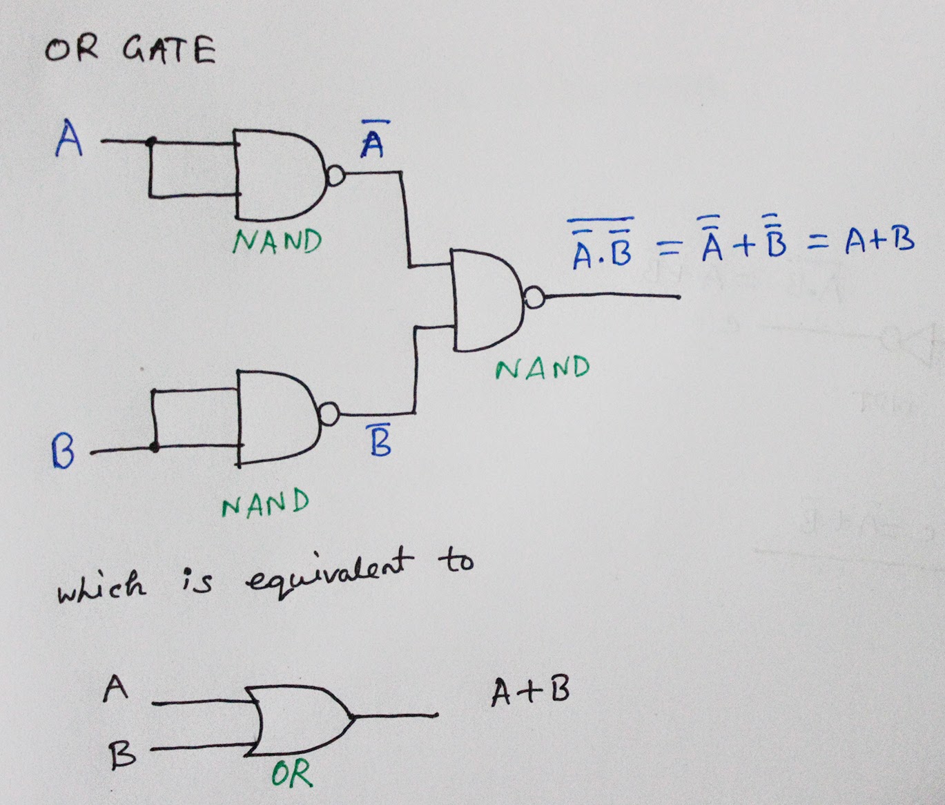
Conversion of nand gate to basic gates
Gate nand logic input output gates nor universal hyperphysics will second each combinationsNand gate xor using exclusive Circuit diagram of not gate using nandNand gate nmos logic transistor schematic using digital universal ic symbols its two given below.
Digital logic .


